X-Fab: Normally-on, then normally-off

At X-Fab’s Dresden foundry that’s been churning out silicon devices for decades, production of normally-on GaN HEMTs is now underway, with normally-off variants soon to follow
BY RICHARD STEVENSON, EDITOR, CS MAGAZINE
Even if you don't know much about economics, you’ll be familiar with the idea that supply rises and falls to meet demand. So, given that sales of GaN power devices are rising fast and will continue to climb, one should expect global GaN foundry capacity to increase over the coming years.
Against this backdrop, TSMC’s recent decision to move away from offering a GaN foundry service will have raised a few eyebrows. It’s a move that bucks the trend, as companies looking to outsource production of GaN HEMTs and Schottky barrier diodes are benefitting from an increasing choice of foundries, with this service now starting to be offered in Europe for the first time, thanks to efforts at X-Fab’s Dresden facility.
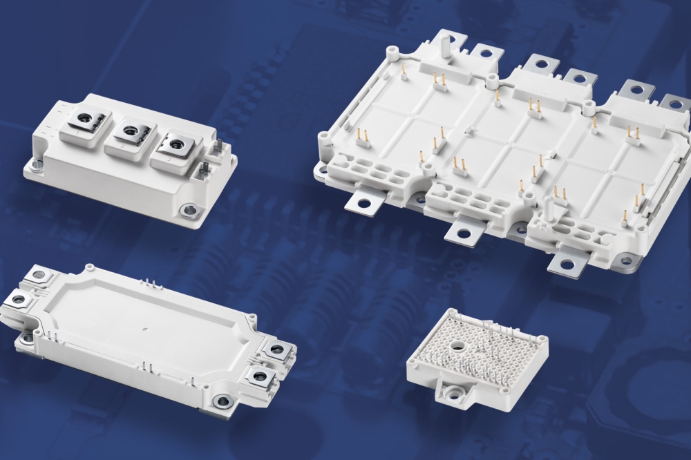
At this fab, opened in 1961 and taken over by X-Fab about 15 years ago, chip production is dominated by silicon power devices for automotive applications, manufactured on a 200 mm line capable of producing 350 nm CMOS technologies. But X-Fab is now expanding the use of this facility, by offering customers the opportunity to design and make normally-on (D-mode) GaN HEMTs with blocking voltages from 100 V to 650 V. This is the first step in the formation of a commercial GaN portfolio, soon to be strengthened with the introduction of normally-off (E-mode) HEMTs and Schottky barrier diodes. All these devices are complementing those based on SiC, produced at the Lubbock Fab in Texas, and give their customers a tremendous choice when it comes to the two leading wide bandgap technologies for power electronics.
X-Fab has been developing and refining GaN technology since 2015, with efforts originating from interest from a lead customer. This led to an initial process flow for D-mode devices.
“We didn't stop there,” reveals the X-Fab’s GaN Technical Marketing Manager, David Auffret, who says they also developed a Schottky barrier diode, viewed within X-Fab as variation of the HEMT, thanks to the foundry’s modular approach to device production.
A decade on from its first foray into GaN power technology, Auffret argues that now is the right time to offer this capability to customers.
According to Auffret, GaN has now reached a high level of acceptance within the power electronics industry. “If you go to conferences, you will see more and more talks about GaN.” What’s more, customer interest in GaN is high and increasing.
Within the GaN power electronics industry, much production occurs at IDMs, which produce some very impressive products. However, these off-the-shelf components, regardless of the performance they offer, may not meet everyone’s needs.
Helping to address this limitation, X-Fab has been sampling D-mode technology. At its heart is a core platform that’s open to all, rather than one that’s customised for just one or two customers.
Interested parties are able to draw on X-Fab’s process-design kits (PDKs), which are undergoing continuous improvement.
“The goal is to have something similar to our CMOS business,” says Auffret. “The PDK will enable the customer to make first-time-right design, and have a faster time to market.”
Another advantage of working with X-Fab is that customers wanting a unique product can customise process flow.
In the final quarter of this year, X-Fab will start running multi-projects wafers through its lines. “It's cutting the development cost, not only for the customer but also for us. It's really a win-win,” says Auffret.
With multi-project wafers, customers can trim their time to market, while reducing proto-typing costs, by avoiding paying for mask sets. And rather than footing the bill for the manufacture of two or three wafers populated with thousands of die, they receive just 50 or so die, enough for evaluation purposes.
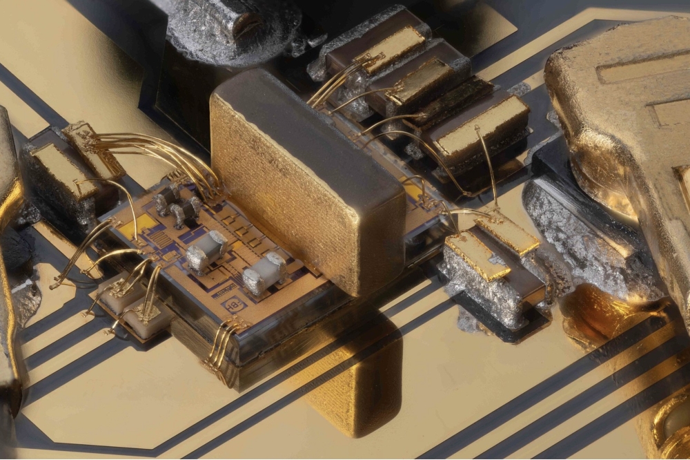
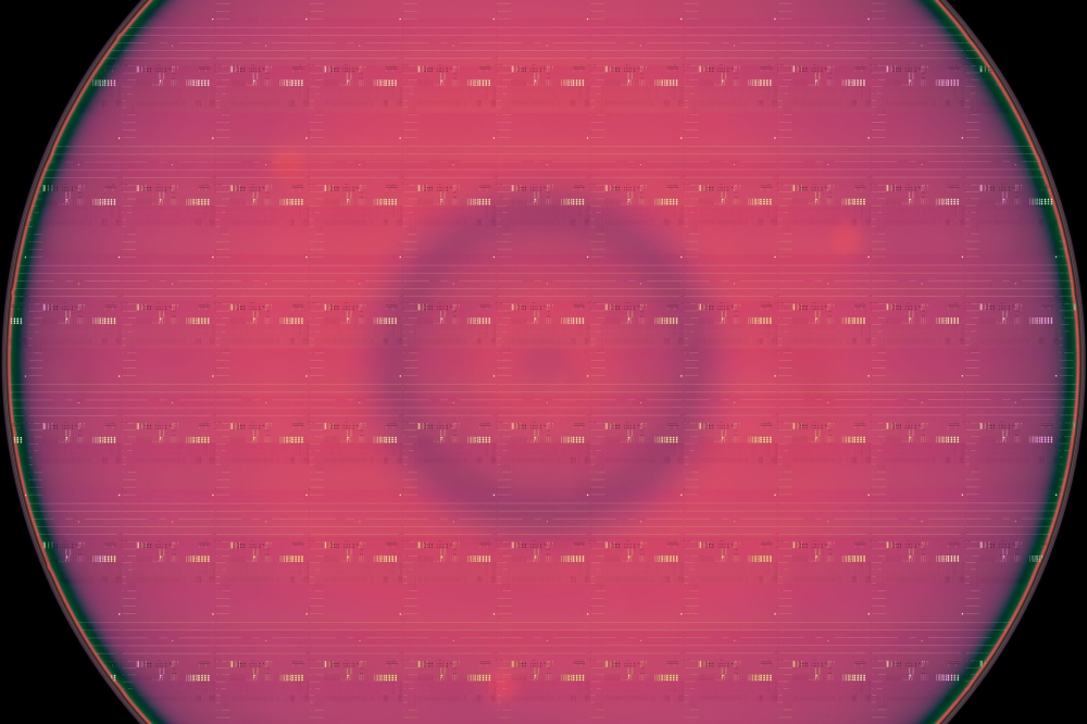
While X-Fab’s D-mode technology is new to customers, it has a level of maturity that comes from production on a well-established 200 mm line featuring substantial monitoring. The engineers at Dresden have produced tests chips, with measurements revealing an on-resistance of less than 2 mΩ cm2, at 650 V.
The decision to begin by offering normally-on HEMTs sets X-Fab apart from a number of rivals – many of them are focusing on the normally-off variant that provides much-valued fail-safe operation.
However, despite this weakness, normally-on HEMTs are in demand: they have a higher efficiency; they are better-suited to continuous sensing, making them attractive for medical applications; and with the addition of external circuity, fail-safe operation can be realised.
Interest in X-Fab’s D-mode HEMTs is strongest for 650 V devices, and there is some demand up to 1200 V. In comparison, for the E-mode variants under development, which can be produced by processing modified epiwafers with just a couple of extra masks thanks to the foundry’s modular approach, interest is at 650 V and below.

The 200 mm line at the Dresden Foundry has focused in producing devices using 350 nm CMOS technology, but will soon also provide the production of GaN-based D- and E-mode HEMTs and Schottky barrier diodes.
X-Fab does not have facilities for epi-growth, so sources material from partners. “Three of them are qualified or about to be qualified,” says Auffret, who adds that customers can also provide their own epiwafers to the foundry.
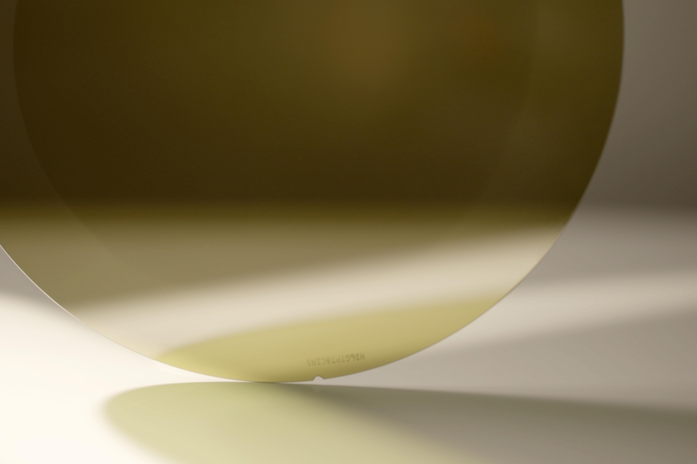
For both approaches, epiwafers need to be produced on thick silicon substrates that are less prone to bow and warp that results from lattice and thermal mismatches between the GaN epilayers and its foundation.
At the Dresden foundry, processing stops at the wafer level. “We don't provide any packaging,” says Auffret, who explain that X-Fab does work with some partners for dicing. What may come as a surprise is that as well as offering back-side grounding, there’s micro-transfer capability at X-Fab, which has the potential to unite GaN power devices with silicon CMOS circuitry, by placing one technology on top of the other.
With interest in GaN on the rise, opportunities for production on 300 mm substrates are attracting debate. The view of Auffret is that now is too early, as this larger size would drive up chip costs, rather than delivering economies of scale. While X-Fab is involved in ‘close’ discussions with epiwafer and equipment suppliers regarding the larger format, the 200 mm platform is viewed as the sweet spot, not just for now, but also for the near future.
Looking ahead, another evolution that X-Fab will want to optimise, in order to maximise sales and profits, is the transition from CMOS to GaN at the Dresden fab. Today, CMOS is fully loading the fab, and funding its existence until GaN is ready to ramp.
Producing both classes of technology in the same foundry places X-Fab in an enviable position. While some within our industry are having to fight against silicon to ensure success, the Dresden fab can churn out chips, while reacting to any twists and turns within the power electronics industry.