Wolfspeed: Making material gains
The pioneer of SiC starts to offer 200 mm substrates and epiwafers to all.
BY RICHARD STEVENSON, EDITOR, CS MAGAZINE
For the last year or so, Wolfspeed has been in the news for the wrong reasons. Recent coverage of this SiC specialist has focused on its crippling debt, a filing for Chapter 11 Bankruptcy protection, and a global market softness that holds back its exploitation of a vastly expanded production capacity. These ferocious headwinds have caused the company to lay off many staff, and are behind a share price that’s fallen through the floor.
However, over the last few weeks Wolfspeed has started to change the narrative. Helping to drive this are a filing of positive press releases: one details a financial restructuring process that has enabled the company to emerge from Chapter 11 protection and substantially reduce its debt – a good move, but one that’s been very, very hard on existing shareholders; and another outlines the opening up of its 200 mm substrate and epiwafer expertise to all.
In the halcyon days of the SiC industry, when global substrate supply struggled to keep pace with demand, Wolfspeed signed a handful of substantial wafer supply agreements totalling around $2 billion. These deals enabled the likes of Infineon, STMicrolectronics, onsemi, and Rohm to secure 150 mm SiC substrates from the world’s leading supplier.
Last year Wolfspeed started to expand this side of its business by offering its 200 mm substrates to selected high-volume customers, while fine-tuning material specifications. And now it’s gone one step further, opening up this product to all.
According to Cengiz Balkas, Wolfspeed’s Chief Business Officer, this latest step reflects the company’s readiness to supply the industry with the quality and volumes of 200 mm SiC that will be needed.
“We've gone through these wafer transitions many times in our history,” says Balkas, who explains that migrations from one diameter of substrate to a larger variant always begin with internal use of the larger size. “Once we go through that initial heavy lifting of getting everything settled in, we come to market and start ramping our commercial customers.”
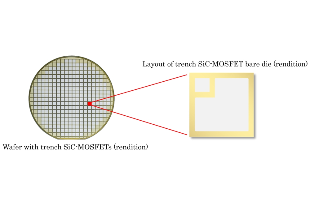
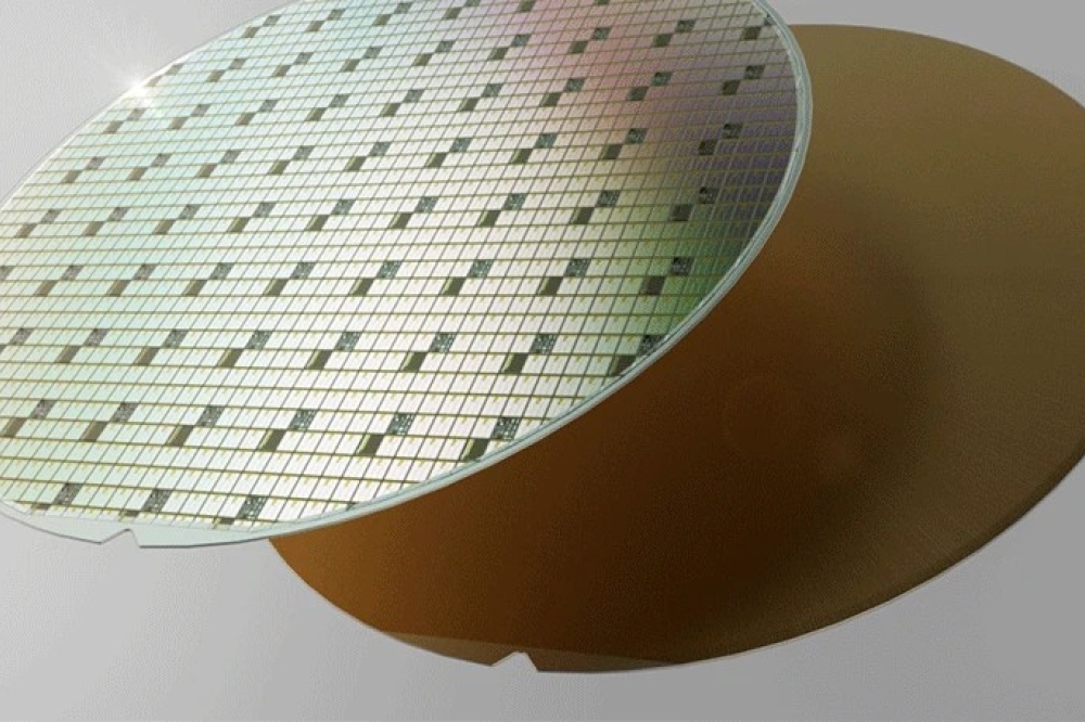
For the company’s 200 mm format, substrates are manufactured at its historic facility in Durham, North Carolina, with production of SiC MOSFETs and Schottky barrier diodes undertaken at the device factory in Mohawk Valley, New York.
As Wolfspeed is the largest consumer of 200 mm substrates, used to make its 600 V, 1200 V and 1700 V SiC MOSFETs and Schottky barrier diodes, it’s of no surprise that the majority of this material is deployed for internal chip production. “But we definitely have enough volume to start ramping our customers,” says Balkas.
Quantity and quality
Any chipmaker that uses Wolfpseed’s 200 mm substrates will not trade a larger size for inferior quality. “They're definitely better than our 150 mm wafers millimetres,” says Balkas, explaining that they have lower densities of micropipes, screw dislocations and basal place dislocations, as well as a lower residual stress and better surface parameters.
Improvements in material quality will continue at Wolfspeed, and while efforts are focused on the 200 mm format, insights into how to produce better boules will be applied to the manufacture of 150 mm products.
For all forms of SiC substrate, Wolfspeed will be following the well-known pathway for the semiconductor industry, making substrates better and cheaper over time. According to Balkas, the cost-per-unit area of the company’s substrates is on a “pretty significant reduction curve”.

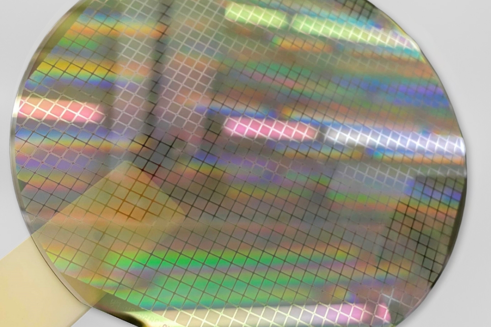
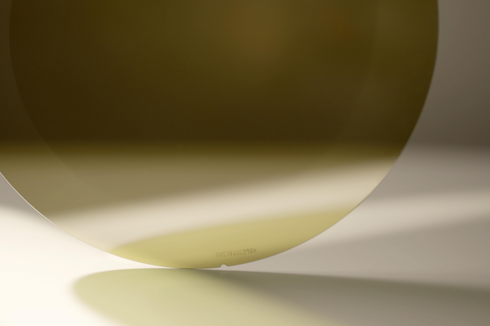
The uniformity in the cross-polarised image underscores the quality of Wofspeed’s 200 mm substrates.
Prices that customers pay for this format are confidential, and will depend on volume. It’s possible that those switching from 150 mm to the larger format will initially pay more per-unit-area when ordering small quantities to get going, but as volumes increase for both the customer and Wolfspeed, the larger format will be the more economical one.
Spurred on by the growth of the SiC market, more companies are producing substrates, with Wolfspeed facing particularly fierce competition from China. According to the market research firm Yole, Wolfspeed is still the clear leader in this sector, but its market share is in decline.
In any market, rivals always look for factors that allow them to stand out from the crowd. Viewed in these terms, Balkas believes that Wolfspeed’s vertically integrated approach gives it a crucial edge.
“We make automotive-qualified power devices in our New York factory,” says Balkas, who points out that this allows Wolfspeed to have a credible case when customers consider placing orders for 200 mm substrates.
A number of producers of SiC substrates are looking to raise their profile by showcasing 300 mm substrates. While this is an impressive feat, it is far from clear how long it will be until high-volume production of SiC power devices even begins on 300 mm lines.
“For us, next steps are to get through the 200-millimetre transition and ramp the industry on 200-millimetre. It looks pretty early to me to discuss 300-millimetre,” argues Balkas.
Outsourcing epitaxy
Within the wide bandgap power electronics industry, many of the producers of GaN HEMTs are fabless, while the SiC sector is dominated by those with their own production lines.
Given this, one may not expect much demand for SiC epitaxy. But there is, and always has been, according to Balkas.
“What we see, especially in the early stages of a diameter change, is that our customers really have a need for epi services. If I look at the 150 mm-millimetre long-term agreement, we had a significant amount of 150 volume – that was a combination of availability of epi, quality of the epi, and the pricing that we can offer.”
For epitaxy on 200 mm SiC, Wolfspeed offers thickness and doping uniformities of ± 8 percent and ± 12 percent, respectively as baseline specifications – figures derived by considering all points within an area that’s defined by edge exclusions of 3 mm for usable area, and 4 mm for doping uniformity. Useable area is more than 85 percent, for a 5 mm by 5 mm grid.
Those impressed with these figures and interested in securing these epitaxial services should have no concerns whatsoever related to Wolfspeed keeping their IP completely confidential.
“We're extremely proud of our history and reputation in the market,” says Balkas, who reveals that the company has multiple protection rules to prevent any customer information relating to their epiwafer design from reaching those within the company that work on Wolfspeed’s own devices. “Our track record is spotless.”
By combining epitaxial services on 200 mm SiC with substrate access to all, Wolfspeed is in a great position to lead this industry’s production of power devices on the larger format. It’s a significant milestone that will be welcomed by producers of SiC MOSFETs and Schottky barrier diodes. But only time will tell how much this will do to help to revive the fortunes of Wolfspeed, and fill its vastly expanded capacity.