Improving MBE for GaN power devices
A team from China has strengthened the case for manufacturing GaN HEMTs by plasma-assisted MBE by producing simple devices that can block more than 2.5 kV.
While MOCVD dominates the manufacture of GaN HEMTs for power electronics, there are a number of benefits associated with plasma-assisted MBE.
One of the strengths of this class of epitaxy is that it is capable of producing an insulating buffer without the need for doping. Avoiding doping is a significant asset, as it eliminates current collapse when switching GaN HEMTs between their on and off states.
Another advantage of plasma-assisted MBE is the suppression of background impurities and defects, thanks to growth under ultra-high vacuum.
Exploiting these assets, the team from Massphoton, Suzhou Powerhouse Electronics Technology, and Suzhou Institute of Nano-Tech and Nano-Bionics, have produced GaN HEMTs that feature a 70 nm-thick channel produced with a novel growth scheme.
To form this device, the team divides the growth of the channel into 12 layers and employs a gallium droplet depletion treatment. This approach is said to enhance the quality of the GaN channel, due to fewer defect states and a lower pore defect density.
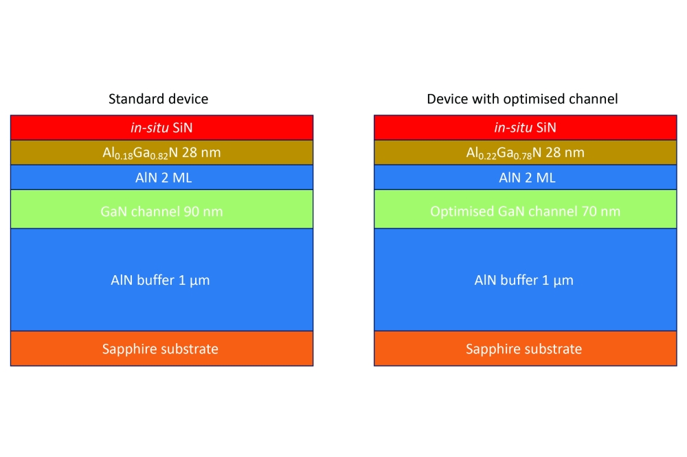
Fabrication of the HEMTs began by loading a 3-inch sapphire substrate with a 2 ° off-cut into a plasma-assisted MBE chamber and depositing a 1000 nm-thick AlN buffer at 920 °C, followed by growth of the 70 nm-thick GaN channel, two monolayers of AlN and a 28 nm-thick layer of Al0.22Ga0.78N, all at 815 °C. After growing this III-N stack, the team added, in situ, a 10 nm-thick SiN passivation layer. In addition, the team produced a control device with a slightly thicker channel (see Figure for details).
Processing these epiwafers into devices began with the deposition of a 30 nm-thick SiN layer by low-pressure CVD, followed by nitrogen implantation to realise mesa isolation, and the addition and annealing of source and drain ohmic contacts. After the growth of a 150 nm-thick layer of SiN, gate windows with a recess depth of 120 nm were defined, to leave 30 nm of SiN as the gate insulator. Deposition of Ti/Al/Ti followed, creating a gate metal and field plate, prior to the addition of interconnects and deposition of a 2 µm-thick SiN top passivation layer.
Electrical measurements using the transmission line method determined a contact resistance of 3.6 Ω mm and a sheet resistance for the wafer of 491 Ω sq-1. Meanwhile, Hall measurements provided values for the two-dimensional electron gas density of 1.07 x 1013 cm-2 and the field-effect mobility of 884 cm2 V-1 s-1, suggesting a sheet resistance of 660 Ω sq-1. The engineers attribute a discrepancy between values for sheet resistance obtained from different measurements to a buffer layer below the GaN channel that’s not sufficiently insulating and leads to parasitic conduction.
It’s claimed that improving the growth conditions of the buffer layer would reduce the sheet resistance and enable a thicker channel layer.
Transfer measurements of the GaN HEMT featuring modified channel growth show current saturation in the output characteristics. This characteristic, not observed in a control device with a conventional channel, is attributed to the superior channel produced with subdivided layers.
Additional benefits associated with the superior channel include an increase in the on-off ratio to 107 and a reduction in the drain leakage current at a drain bias of 0.5 V to 1 nA mm-1 – in both cases, there is an order-of magnitude improvement over the HEMT with the conventional channel.
Both forms of HEMT have a relatively high on-resistance, due to the thin GaN channel thickness.
According to the team, increasing the channel thickness will help to reduce the on-resistance, which can also fall by introducing a graded layer and improving the growth process.
The control device breaks down at 1000 V, while the HEMT with the superior channel can withstand around 2500 V. The team speculates that the far higher value stems from the superior insulating properties of the GaN channel.
Pictured above: A superior channel improves the HEMT’s blocking voltage, leakage current and on-off ratio.
Reference
Z. Yang et al. Appl. Phys. Express 18 114001 (2025)