Giving ß-Ga₂O₃ an insulating buffer
Researchers from the University of California, Santa Barbara (UCSB), are claiming to have developed a superior process for addressing an unintentional silicon peak in ß-Ga2O3 heterostructures.
This peak, occurring at the interface between ß-Ga2O3 substrates and homoepitaxial layers, degrades device performance in a number of ways. One downside of the silicon peak is that it creates a low-mobility electron channel further from the gate terminal that adds to delays associated with resistance and capacitance, and ultimately hampers fast switching and high-frequency performance in lateral devices. In addition, the peak leads to a higher pinch-off voltage and an increased subthreshold slope; and it can increase leakage and lead to premature breakdown.
Back in 2023, a collaboration between UCSB and the University of Utah reported that it’s possible to remove the silicon peak by dipping the substrate in 49 percent hydrofluoric acid prior to growth. However, this process is time-sensitive, with the peak returning in around 10 minutes under ambient exposure.
Now, Sriram Krishnamoorthy and co-workers are arguing that they have developed a superior process, involving growth, by MOCVD, of an insulating buffer that compensates the interfacial charge.
According to the team, the benefits of the insulating layer extend beyond charge compensation to include aiding the performance of vertical and lateral FETs. It is said that the addition of the buffer offers an advantage in vertical devices, as it allows the inclusion of wider fins in vertical enhancement-mode devices, by creating a potential barrier in the fins.
The insulating buffer could act as a current-blocking layer, using acceptors such as nitrogen, magnesium or iron. A major merit of nitrogen is its deep acceptor level, 2.9 eV below the conduction band, that reduces the likelihood of inadvertent activation. The acceptor level for iron is not as deep; and while that’s not an issue for magnesium, its weakness is that it lingers in the reactor, and is unintentionally incorporated in epilayers in subsequent growth runs.
To investigate the impact of a nitrogen-doped buffer, Krishnamoorthy and co-workers have grown a number of samples in an Agnitron Agilis 1000 vertical cold-wall reactor. Prior to growth, iron-doped (010) ß-Ga2O3 substrates were cleaned in acetone, methanol and deionised water. Omitting the etch in hydrofluoric acid allowed the team to see if the nitrogen-doped layer compensated for the silicon peak.
The researchers grew the nitrogen-doped layer at 910 °C, as higher temperatures reduce the level of hydrogen, which is predicted to cause compensation of nitrogen and act as a shallow donor. What’s more, experiments show that the incorporation of hydrogen roughens the surface of ß-Ga2O3 epilayers.
After growing the nitrogen-doped layer, the team shut off ammonia flow and added a 150 nm-thick silicon-doped layer with an intended doping of 5 x 1017 cm-3.
When growing the nitrogen-doped buffer layer, it’s crucial to hit a sweet spot. Too much nitrogen degrades the crystal quality of the buffer layer, and may increase unintentional impurities in the silicon-doped channel, if there's surface segregation or nitrogen diffusion into active channel layers. But if nitrogen flow is insufficient, there will be incomplete compensation of unintentional silicon impurities.
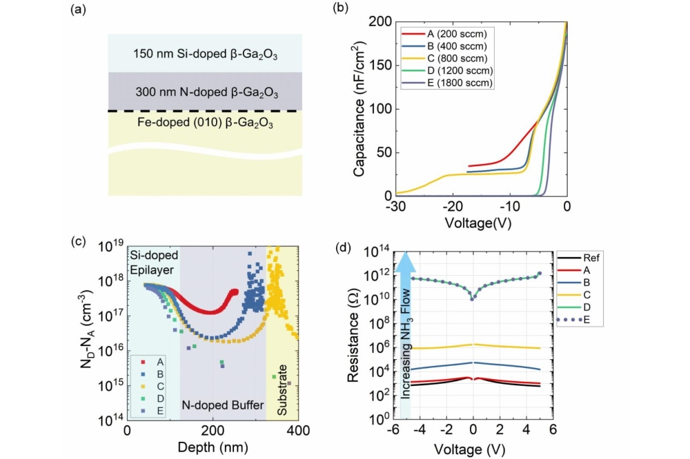
To establish optimal flow, the team produced samples with a range of ammonia/nitrogen flows.
Capacitance-voltage measurements on these samples determined that an ammonia flow rate of 1.8 x 10⁻⁶ mol min-1 provided partial compensation, while flows of 2.7 x 10⁻⁶ mol min-1 and 4.0 x 10⁻⁶ mol min-1 both showed no carrier spike at the interface, indicating that the concentration of nitrogen in the buffer layer exceeds that of silicon at the interface.
To verifying full compensation, the team also produced buffer leakage structures. Measurements determined that as ammonia flow increased, so did resistance.
To quantify the concentration of nitrogen in these structures, the team produced a test structure, based on alternating layers of unintentionally doped Ga2O3 and nitrogen-doped Ga2O3 at various flow rates. According to secondary ion mass spectrometry, nitrogen levels in layers with flows of 2.7 x 10⁻⁶ mol min-1 and 4.0 x 10⁻⁶ mol min-1 are 1.7 x 10¹⁹ atoms cm-3. As nitrogen is not thought to saturate at this level, the constant value is attributed to growth variation.
Based on these results, the team has determined an optimum flow of 2.7 x 10⁻⁶ mol min-1. They have also investigated the optimum buffer thickness, which is 50 nm, according to plots of capacitance versus voltage.
Pictured above: (a) Epitaxial structure of Si-doped channel layer with N-doped buffer (b) C-V and (c) charge density profile of samples with ammonia flows ranging from 200-1800 sccm (d) Buffer leakage compensation data as a function of ammonia flow rate, where Ref is an ohmic pad contacting the Si-doped channel.
Reference
R. Kahler et al. Appl. Phys. Lett. 128 202103 (2026)