Advancing 800 VDC architectures with all-GaN technology
As AI workloads scale to megawatt racks,
GaN’s blend of performance, efficiency, and manufacturability establishes it as
the indispensable technology for powering the next generation of AI
infrastructure.
By Pengju Kong, Jianping Wang, Yi Sun, Jinghua Ni, Huaifeng Wang, Yulin Chen, Charles Bailley and Lei Wu at Innoscience
The explosive growth of AI computing is driving a fundamental transformation in data center power architectures. NVIDIA’s next-generation AI factories adopt an 800 V direct current (800 VDC) backbone to deliver megawatt-scale power with high efficiency and reliability. This shift imposes stringent demands on power devices. While silicon MOSFETs are approaching their physical limits, GaN high-electron-mobility transistors (HEMTs) offer superior performance with ample headroom for further innovation. In response to such demand, Innoscience is collaborating with NVIDIA to develop All-GaN power conversion solutions from 800V to GPU, which supports the 800 VDC power architecture. This paper analyzes the architectural challenges of 800 VDC AI systems and demonstrates why GaN’s device physics, scalability, and manufacturing maturity make it the optimal and future-proof choice for AI-era power delivery.
Introduction
An 800 VDC architecture enables the safe and efficient delivery of megawatt-scale rack power with reduced material and infrastructure costs. However, a major challenge remains: delivering such high power to GPUs within the limited space of a rack server. Advances in power device technology are critical to overcoming this challenge.
Challenges for power conversion to GPU in 800 VDC systems
Compared to a 54 V busbar, power conversion from 800 VDC to the GPU presents significant challenges. The high voltage conversion ratio traditionally results in larger, less efficient power converters—an unacceptable tradeoff for AI systems. Breakthrough technologies are required. Devices must switch at least 10× faster to shrink magnetics and capacitors, while also minimizing conduction loss to reduce heat and conserve valuable board area.
The advantage of GaN power device
GaN’s intrinsic material and device-level properties uniquely position it to meet NVIDIA’s demanding 800 VDC requirements.
The core strength of GaN HEMTs lies in their GaN/AlGaN heterostructure, which creates a two-dimensional electron gas (2DEG) at the interface. This structure provides exceptionally high electron mobility and low parasitic capacitance, yielding reduced gate charge and superior switching performance. It eliminates minority carrier recombination issues, such as the reverse recovery losses seen in silicon MOSFETs, making GaN particularly effective at high switching frequencies. Additionally, GaN’s wide bandgap supports high breakdown voltages with low specific on-resistance. These material advantages translate directly into lower on-resistance, reduced gate charge, and superior efficiency, enabling higher-frequency operation and greater power density in converters. Figure 1 [1] compares the RON, SP (Ron times die size) of Si, SiC MOSFET and GaN. GaN shows significantly lower physical limit compared to Si and SiC MOSFETs, indicating its superior advantage in reducing device size and parasitic capacitance at the same Ron.

Figure 1. Physical Limits of Power Device RON, SP [1]
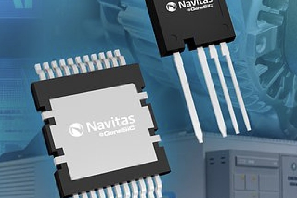
Among GaN technologies, GaN-on-Silicon stands out as the most mature and cost-effective solution. It leverages well-established silicon manufacturing processes and equipment, enabling high-volume scalability while maintaining a competitive cost structure compared to conventional silicon power devices.
The All-GaN solution for 800 VDC and its performance advantage
A three-stage power conversion example, shown in Figure 2, illustrates the advantages of the All-GaN solution for 800 VDC. Innoscience provides a broad portfolio of GaN products spanning 15 V to 1200 V ratings, enabling an All-GaN architecture for power conversion from 800 VDC to the GPU. Specifically, the recommended component selection is listed in Table 1 below.

Figure 2. 800 VDC to GPU Power Conversion Block example and Innoscience All-GaN Solution [2]

Table 1. Topology and Component Selection for 800 VDC Power
800V – 54V using 650V and 100V GaN HEMT
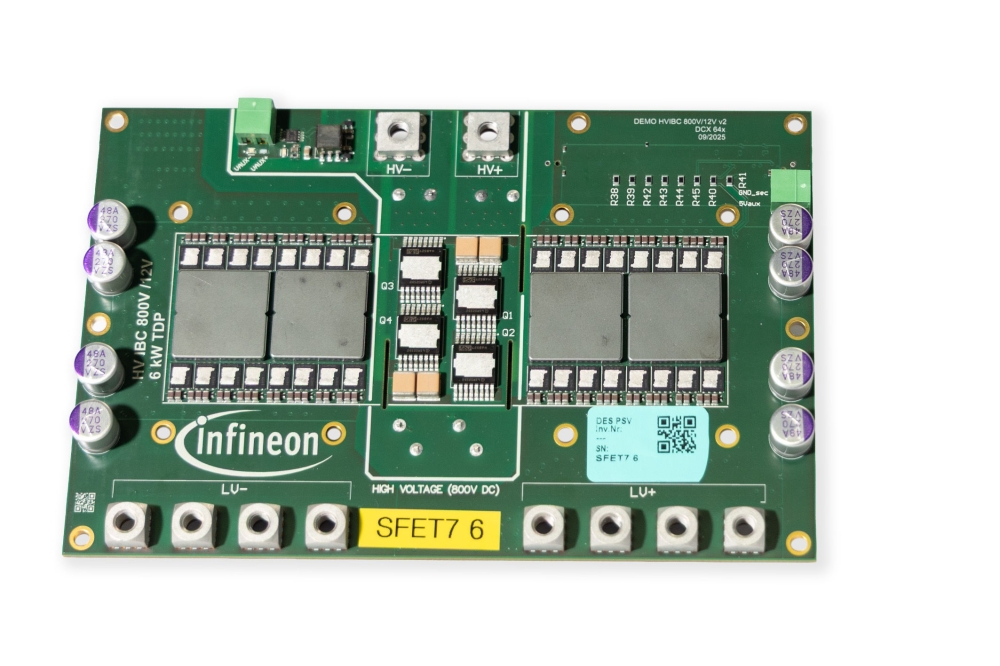
The 800 V to 54 V conversion stage is unique to 800 VDC architectures, making board size reduction a top priority. Achieving this requires both compact magnetics and high-performance power devices. Figure 3 demos the ultra-compact design of a 6kW 800V – 54V converter (power devices and transformer portion only) with targeted 99% peak efficiency using Innoscience All GaN solution.

Figure 3. 800V – 54V Conversion with Innoscience All-GaN solution
The benefits of such solutions include:
- Innoscience 650V GaN HEMTs feature ultra-low input capacitance (Qg) and driving voltage, achieving merely 20% driving loss of a SiC MOSFET, which enables 1 MHz switching without driver overheating.
- Low Qg further minimizes the turn-off loss (Eoff), allowing easier thermal handling at high switching frequencies.
- Innoscience 100V GaN HEMTs are available in 5x6 dual-cool packages as low as 1mΩ (INN100EBD010EAD), which reduce component count and board area by 50% compared to the 2mΩ silicon MOSFETs.
- Low Qg of 100V GaN cuts driving losses by 80%, further supporting high-frequency designs with compact auxiliary supplies.
54V – 12V using 100V GaN HEMT
Converting 54 V to 12 V using traditional 100 V silicon MOSFETs incurs significant reverse recovery and drive losses, forcing designers toward complex and expensive resonant converters. In contrast, Innoscience’s 100 V GaN HEMTs eliminate reverse recovery loss and reduce drive loss by 80%, enabling simple multiphase buck converters to achieve higher power density.
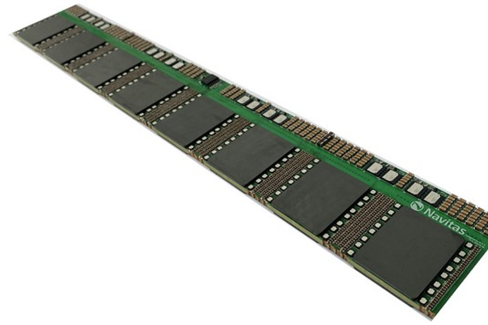
Figure 4 demonstrates a 12kW Power Distribution Board with Innoscience GaN HEMTs. Comparison between GaN and Si MOSFET was done on the same board as they are pin-2-pin compatible. Efficiency of GaN is more than 1% higher, allowing more power delivery. At the same 115C operation temperature, GaN delivers 1.918kW while Si MOSFET only achieves 1.56kW.

Figure 1. Physical Limits of Power Device RON,SP
12V – 1V using 25V GaN HEMT
Innoscience has demonstrated that 30 V GaN HEMTs deliver higher efficiency than the most advanced DrMOS solutions at 2X switching frequency.
Next-generation low-voltage GaN devices will further reduce Rds(on) and switching loss, driving even greater power density for conversions such as 12 V–1 V or 6 V–1 V. 5.
Maturity and reliability of GaN power devices
GaN power device industry has now reached its time for mainstream adoption and readiness for AI era, with almost all major power semiconductor suppliers offering GaN solutions.
Innoscience has been the pioneer and in the leading position with its world’s largest manufacturing capacity, accumulated shipment and reliability data, as well as the understanding on how to make a reliable GaN product for AI and EV applications.
Manufacturing capacity and accumulated shipment
Innoscience is the world’s first and largest 8-inch GaN-on-Si IDM, with capacity projected to reach 72,000 wafers per month by 2027. To date, the company has shipped over 1.5 billion GaN power devices at 95%+ yield, across consumer, industrial, data center, and automotive markets, consistently delivering low defect rates and proven reliability.
Reliability
Innoscience ensures GaN product reliability through rigorous design practices and extensive qualification. Each technology platform maintains significant margin between actual operating loads and fundamental device limits. For example, destructive breakdown voltage testing confirms wide safety margins, as illustrated in Figure 5.

Figure 5. 54V – Load and Stress of drain voltage for an Innoscience technology platform.
Beyond industry-standard qualifications, Innoscience extends test times (2000-hour HTOL), broadens conditions (175oC), and expands test categories to define reliability boundaries. Datacenter-specific tests, such as 1000-cycle temperature cycling on 16-layer, 3.1 mm boards, show zero degradation nor delimitation, as illustrated in Figure 6. With millions of device hours logged across wafer, chip, package, and system-level tests, Innoscience has built the industry’s most extensive GaN reliability database, enabling continuous improvement of device robustness.

Figure 6. Electrical measurements and destructive physical analysis (DPA) data throughout the 1000-cycle TCoB test
Innoscience has built a reliability laboratory capable of supporting high volume mass production. The table below shows the device hour and tested sample size that has been completed in the past 3 years. This high throughput helped Innoscience accumulate the largest GaN reliability database in world and continues to improve its reliability to a higher level.

Table 2. EDevice hour/sample size that has been tested in the reliability laboratory
Conclusion
The adoption of 800 VDC architectures in AI data centers represents a decisive step toward higher efficiency, scalability, and future readiness. An All-GaN approach delivers minimal conduction and switching losses across the full 800 V to GPU conversion path, enabling compact, thermally manageable designs with fewer components. As AI workloads scale to megawatt racks, GaN’s unmatched blend of performance, efficiency, and manufacturability establishes it as the indispensable technology for powering the next generation of AI infrastructure.