NoMIS demos 6.5 kV SiC MOSFET
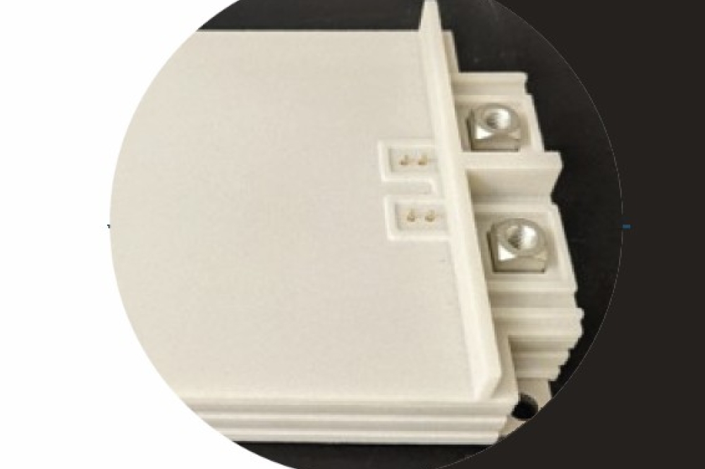
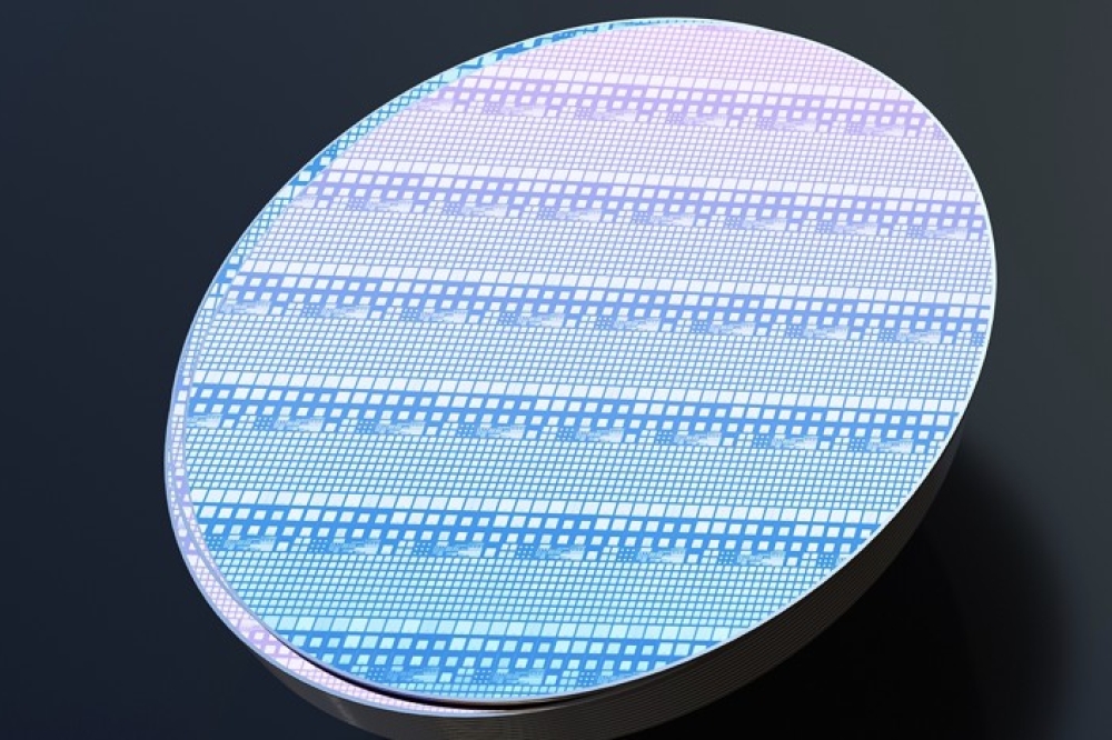
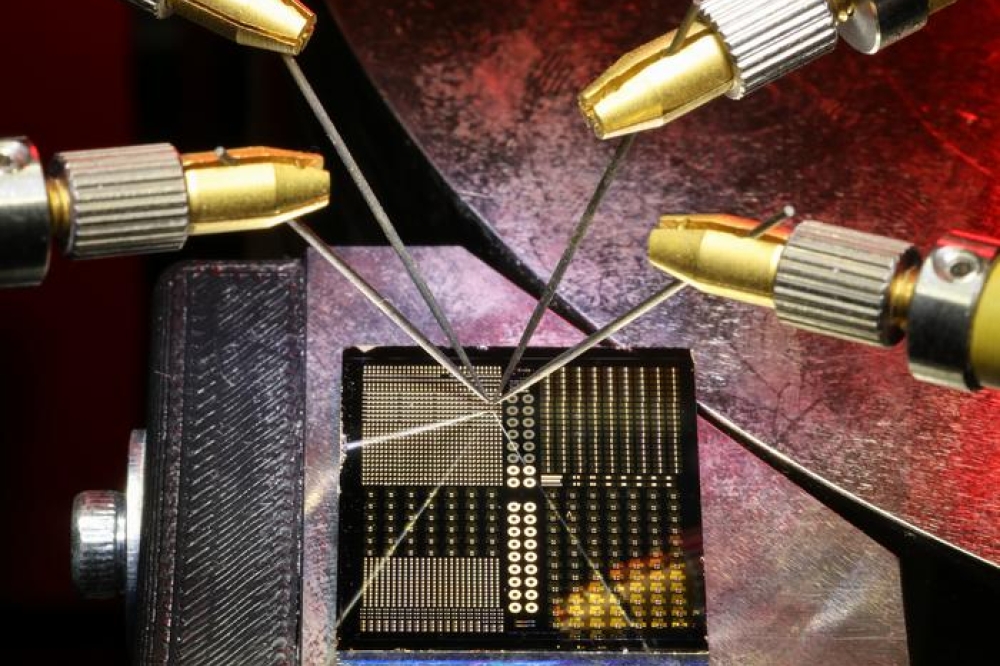
US-based NoMIS Power Corporation, a maker of SiC power semis, has announced the successful demonstration of its first 6.5 kV large-die SiC MOSFET.
The device was measured at over 8 kV blocking, 90 mΩ on-resistance, and 55 A drain current. NoMIS says the result carries its planar SiC device technology from its established 3.3 kV devices into the high-voltage class, and establishes a clear, demonstrated path toward the company's forthcoming 10 kV MOSFETs and 20 kV SiC IGBTs.
Currently, NoMIS Power's high-voltage SiC roadmap spans three stages — 3.3 kV in production and 6.5 kV sampling, with 10 kV in development:
3.3 kV — available now. The complete 3.3 kV SiC MOSFET family is in production, spanning 80 mΩ (34 A), 50 mΩ (55 A), and 25 mΩ (105 A) devices in TO-247-4L-HC and bare die, complemented by 50–160 mΩ SiC bi-directional switches and a 500 A half-bridge power module.
6.5 kV — sampling now to US-based customers. The demonstrated large-die SiC MOSFET is sampling now for evaluation and anchors an expanding 6.5 kV line, adding on-resistance variants, small-die devices, hybrid junction-barrier Schottky FET (JBSFET) devices, and standalone diodes. JBSFET construction prevents body diode degradation issues, making it very robust for critical applications. Target applications include high-voltage direct current (HVDC), solid-state transformers, pulsed power, rail traction, and MW-scale EV charging. Standard production 6.5 kV parts are scheduled for Q4 2026 and will be available to commercial customers.
10 kV and above — in development, sampling in Q4 2026. The pipeline includes MOSFETs, diodes, hybrid (JBSFET) devices, and SiC insulated-gate bipolar transistors (IGBTs) targeting grid-scale HVDC, next-generation traction, and advanced pulsed power, extending the roadmap toward 20 kV.
"Demonstrating 6.5 kV blocking to over 8 kV proves our planar SiC platform scales cleanly from the 3.3 kV devices shipping today into the high-voltage class," said Adam Morgan, co-founder and CEO of NoMIS Power. "High-voltage SiC is becoming foundational to data-center, grid, aerospace, and defence power systems, and it should be built at home — we're building the domestic source the industry can qualify against, from 3.3 kV and 6.5 kV today to 10 kV MOSFETs and 20 kV SiC IGBTs on our roadmap."
The 6.5 kV large-die SiC MOSFET is sampling now to US-based customers for evaluation, with standard production parts scheduled for Q4 2026. NoMIS Power is engaging system developers on design-in, custom current ratings, and packaging. Teams evaluating high-voltage SiC for HVDC, solid-state transformers, pulsed power, traction, high-power charging, or aerospace and defence platforms can contact NoMIS Power to align to the 6.5 kV, 10 kV, and 20 kV roadmap.
NoMIS Power designs SiC devices, packaging, and power modules at its facility within the Albany Nanotech Complex in Albany, New York.